Activity
Seminar
Future of Advanced Semiconductor Packaging: Glass, TGV, HBM, CPO & System Integration seminar - 1
1. Date & Time : June 5, 2026 (Thurs), 10:00 – 17:00
2. Venue : Suwon Convention Center, Rooms 205 & 206
3. Schedule
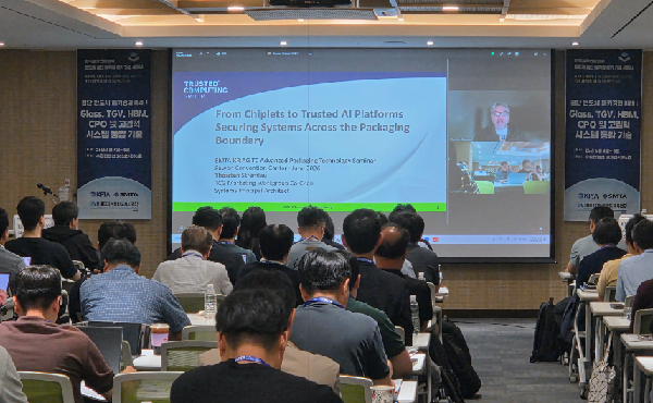
10:00 – 10:40 From Chiplets to Trusted AI Platforms: Securing Systems Across the Packaging Boundary / Thorsten Stremlau / NVIDIA
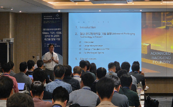
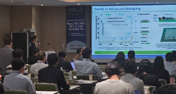
10:50 – 11:30 Trends in Advanced Semiconductor Packaging Technologies / Jong-Heon Kim, Vice President / nepes
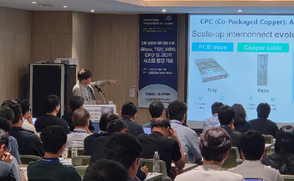
11:40 – 12:20 Challenges and Opportunities in Co-Packaged Optics (CPO) / Kwang-Sung Choi, Director General / ETRI
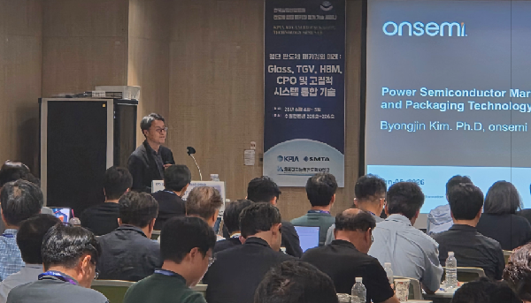
13:30 – 14:10 Market Trends and Packaging Technology Developments for Power Semiconductors / Byung-Jin Kim, Senior Manager / Onsemi
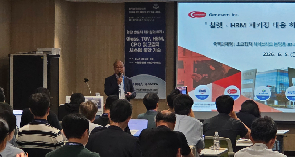
14:20 – 15:00 Hybrid Bonder Technology for Chiplet and HBM Packaging / Jung-Ho Cho, Vice President / Genesem
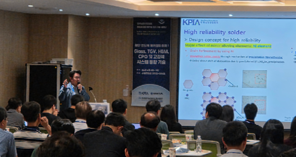
15:10 – 15:50 Changes and Applications of Solder Products in Response to Evolving Semiconductor Package Requirements / Young-Woo Lee, Team Manager / MK ELECTRON
16:00 – 16:40 Development Status of Metallization and TGV Filling Technologies for Glass Substrates / Seok-Bong Oh, Director / MKS Atotech
- New post
- There is no new post.