Activity
Seminar
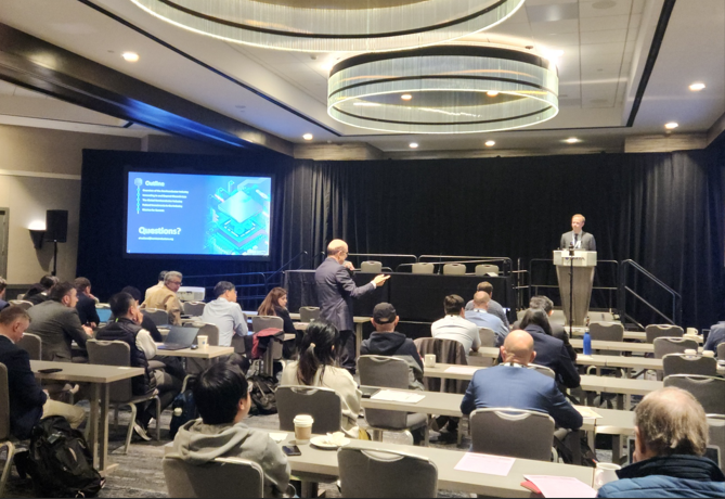
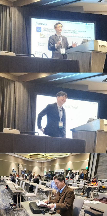
2025 SMTA Wafer Level Packaging Symposium
2025 SMTA Wafer Level Packaging Symposium
- Date : February 18-20, 2025
- Venue : SanFrancisco, CA, USA
<Program>
Professional Development Courses
PDC1:Materials and Processes for the Enablement of Advanced Packaging
PDC2: The Importance of Wafer Level Packaging for the Future of the Semiconductor Industry
Session 1 - Assembly/Integration Process
Laser Assisted Transfer of Coupon of InP Epitaxial Layer for Silicon Photonics Devices
Extension of Die to Wafer & Die to Substrate Fluxless Thermo-Compression Bonding to Panel Level Packaging
A Novel Expansion Process for FO-WLP Using Tape Expansion, Self-Assembly, & Tape Frozen Detachment Technique
Unlocking the Potential of Hybrid Organic-Ceramic Nanocoatings for Chip Packaging
Thin-Film Metal in Redirect Layers: Enabling High-Performance Wafer-Scale Packaging
The CHIPS and Science Act: Past, Present and Future of U.S. Microelectronics R&D
Insights from Nvidia and Semiconductor Industry Association
Session 2- Invited Speakers
Session Chair: YoonChul Sohn, Ph.D., Chosun University
Session Co-Chair: HyunHo Kim, Ph.D., KPIA
In Collaboration with KPIA
Pre-Bond Metrology for Hybrid Bonding: Considerations for High Volume Manufacturing
Novel Electrodeposition Techniques for Through Glass Via(TGV) Process
Session 3 - Substrate/Integration Platform
Session 4 - Novel Bonding and Interconnect Process and Materials
Session 5- Test & Metrology
Session 6 - FOWLP
FOWLP Round Table Discussion
The Future of Panel Level Packaging